PIN Diode-Definition, Characteristics, Structure, And Application
 written by Adeel abbas
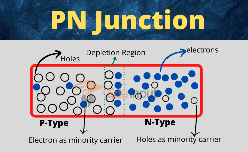
A PIN diode is a diode in which there is a wide, undone intrinsic Semiconductor region between a p-type Semiconductor and an n-type Semiconductor region. The p-type and n-type regions of the pin diodes are heavily doped because they are used for ohmic devices.
The wide intrinsic region is different from the ordinary p–n diodes. The wide intrinsic region makes the PIN diode switches an inferior rectifier, but it makes them suitable for a wide range of power electronics applications.
PIN Diode
Jun-Ichi Nishizawa and his colleagues invented the PIN photodiode in the 1950s. It is a device that is made of Semiconductors.
In the year 1952, the PIN diode was first used as a low and high-power rectifier. It is said to be a good light absorber and was used for microwave applications and as a photodetector.
The p-type Semiconductor and the n-type Semiconductor region are the two regions where a PIN diode is placed. There are applications for ohmic contacts in these two regions.
Characteristics of Pin Diode
There are some important characteristics of pin diode
- The standard equation for low- Frequency signals is obeyed by the PIN diodes.
- The PIN-diode diode looks very linear at higher frequencies.
- The stored charge can be fully swept at low frequencies. There is not much time to sweep the charge from the drift region at higher frequencies.
- The net charge in the intrinsic layer is said to be less than in the bias level, which makes the PIN diode’s capacitance independent of the bias level.
- The depletion region is almost completely within the intrinsic region. The depletion region is larger than in a PN diode and almost constant in size, independent of the reverse bias applied to the diode.
- The high-frequency resistance is related to the DC bias current through the diodes
Pin Diode Structure
The three layers of the P-type layer, Intrinsic layer, and N-type layer are shown in the figure.

The region between the P and N regions consists of a thin layer of material, which is said to be very low in density. The N-type regions are known to be heavily doped.
The changes in the properties of the diodes can be seen from the intrinsic material. Silicon is the material used to make these diodes.
The inferior region of the PIN diode acts like an inferior rectifier and is used in various devices such as attenuators, photodetectors, fast switches, high-voltage power circuits, etc.
Application of Pin diode
In the field of physics, PIN Diode has a wide range of applications like radio Frequency switches, microwave switches, radiofrequency attenuators, microwave attenuators, photodetectors, etc.
These diodes are used in the RF and also for microwave switches and microwave variable attenuators since they are said to have low capacitance. They are used in photodetectors and photovoltaic cells, and the PIN photodiodes are used for network cards and switches.
RF protection circuits can be accomplished with these diodes, and they can also be used as an RF switch. The PIN photodiode can be used to detect X-rays and gamma rays.
Leave a Reply