PN Junction | Forward Biased PN junction and Reverse Biased PN junction
 written by Adeel abbas
A PN junction is formed when a crystal of silicon or germanium is grown in a way that one half is doped with a trivalent impurity (P-type semiconductor) and the other half is doped with a pentavalent impurity (N-type semiconductor).
What is a PN junction?
PN junction is one of the most essential building blocks of electronic devices. It is also used in rectification.
Majority and Minority Carriers in PN junction
An N-type region contains electrons as the majority carriers and a few holes as the minority carriers.
Similarly, the P-type half contains holes as majority carriers and few electrons as minority carriers.
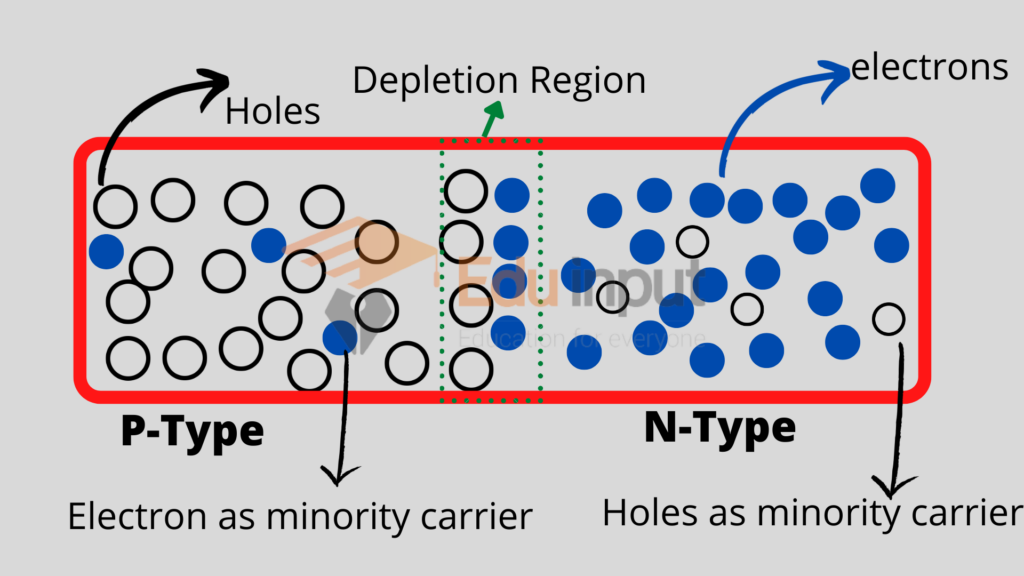
Just after the formation of the junction the free electrons in the N-region, due to their random motion diffuse into the P-region.
Where these electrons combine with the holes in the first layer of the P region and a charge-less region is produced.
This charge-less region around the junction in which charge carriers are not present is called the depletion region the depletion region is formed due to the diffusion of charges
Depletion Region and Potential Barrier:
Due to the combining of the electron-hale pair, the ions on both sides are exposed and they form a potential difference. This is called the potential barrier of the PN junction and it has (0.7 V) for silicon and (0.3 V) for germanium.
This barrier prevents further diffusion of electrons Sol of
Forward biased PN junction
A junction is said to be forward biased when an external potential difference is applied across the PN junction in such a way that the P-side is connected to the positive terminal of the battery and the N-side is connected to the negative terminal of the battery.
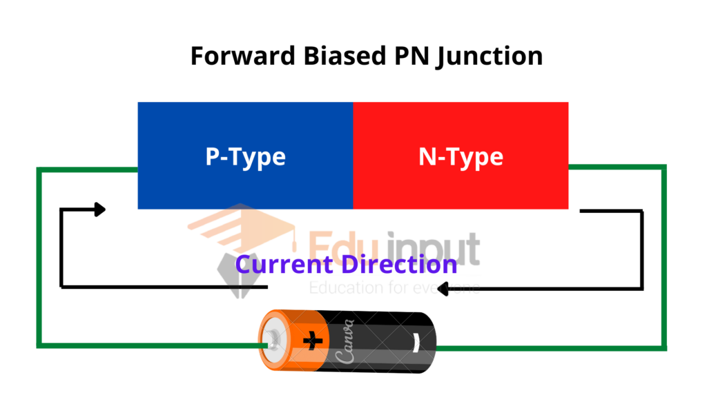
In this connection, the external potential difference supplies energy to both free electrons in the n-region and holes in the p-region.
When the external potential difference is increased from zero, the potential barrier is reduced. At some forward voltage (0.7 V for Si and 0.3 V for Ge) the potential barrier is eliminated and an electric current of the order of a few mili-amperes starts flowing in the circuit.
From the graph, it is clear that if the forward bias voltage is increased by ΔVf the current increases by Δlf.
The ratio of the forward voltage ΔVf to the forward current Δlf is known as the forward resistance of the PN junction and is given by
rf= ΔVf/ Δlf
In forwarding bias, the value of forwarding resistance is very much small in the order of a few ohms indicating that in forwarding bias PN junction offers very low resistance.
Reverse biased PN junction:
In reverse biased, the P-type is connected to the negative terminal and the N-type connected to the positive terminal of the external voltage source.
As a result, the potential barrier at the junction increases. Therefore the junction resistance becomes very high and practically no current flows through the circuit.
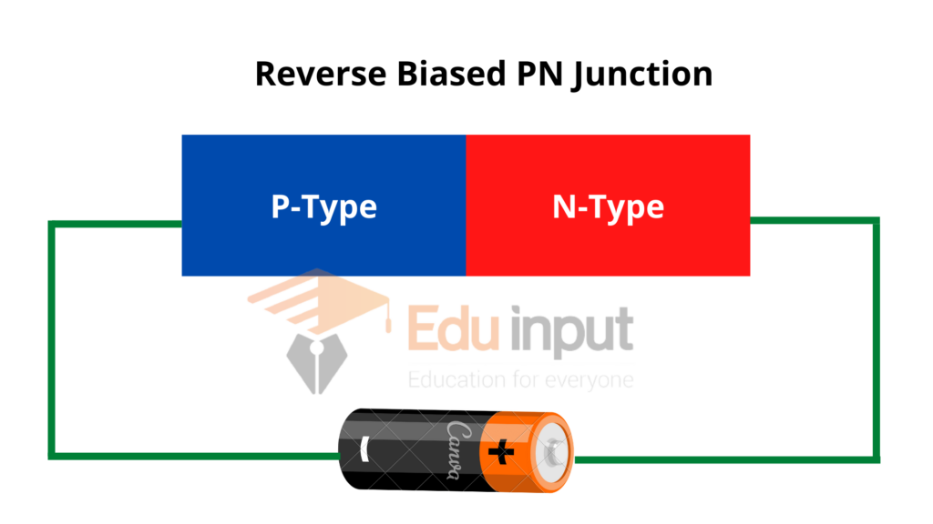
However, a very small current of the order of µA flows in the circuit. It is known as reverse or leakage current
This is called reverse current and is due to the minority carriers because there are some free electrons in the P-type region and some holes in the N-type region. Therefore a very small current flows in the reverse direction
When a reverse voltage is increased from 0 the reverse current quickly rises to its saturation value lo. When a reverse voltage is further increased, the reverse current remains almost constant.
The change of reverse current Δlr is minimal with the change of reverse voltage ΔVr.
Thus reverse bias resistance is given by
rr= ΔVr / Δlr
The value of diode resistance is very high (several mega ohms) with the increase of reverse voltage, and the kinetic energy of minority charge carriers with which they cross the depletion region also increases till is sufficient to break the covalent bond.
As the covalent bond breaks more electron-hole pairs are created. The minority charge carriers increase in number due to which reverse current begins to rise till the junction breaks down.
The reverse current rise sharply and its value is so, high that it can damage the junction.
Semiconductor Diode
A P-N junction is known as a semiconductor diode. The symbolic representation of a semiconductor diode is
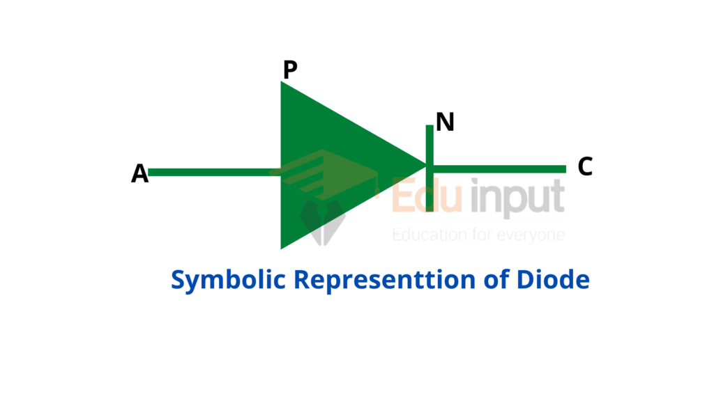
Terminal Naming:
The arrowhead represents the P-region and is also called the anode. The vertical line represents the N-region and is also called the cathode.
Current Direction in Diode:
The outstanding property of a crystal diode is to conduct current in one direction. It conducts current properly when it is forward biased.
Leave a Reply