How zener diode works in reverse bias?
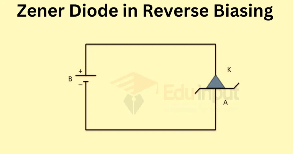
A Zener diode is designed to operate in reverse bias, meaning that the diode is biased in the opposite direction to its normal forward bias. In reverse bias, the P-type material of the Zener diode is connected to the negative terminal of a power supply, and the N-type material is connected to the positive terminal.

In reverse bias, the Zener diode behaves like a normal diode until the applied voltage across the diode reaches a certain value called the Zener voltage. At this voltage, the depletion region of the diode breaks down, allowing current to flow through the diode in the reverse direction. This breakdown occurs due to the avalanche effect or the Zener effect, depending on the doping concentration of the diode.
In the avalanche effect, the reverse voltage across the diode creates a high electric field in the depletion region, which causes electrons to gain enough energy to collide with other atoms and knock out more electrons. This creates an avalanche of electron-hole pairs, which increases the current flowing through the diode.
In the Zener effect, the doping concentration of the P-N junction is carefully chosen to create a narrow depletion region with a high electric field. When the reverse voltage across the diode reaches the Zener voltage, the electric field is strong enough to pull electrons from the valence band of the P-type material into the conduction band. This creates a large number of electron-hole pairs, which results in a sudden increase in the current flowing through the diode.
In both cases, the Zener diode acts as a voltage regulator by limiting the voltage across the diode to the Zener voltage. This makes the Zener diode useful in applications where a stable voltage reference or voltage regulation is required.


Leave a Reply